Solar X-rays:
![]()
Geomagnetic Field:
![]()
From n3kl.org


You may remember in my last post about the bill acceptor project that I had made a preliminary pin count and started assigning functions to the various Arduino pins.
The next step was to input the schematic to Eagle and start laying out the pcb. Capturing the schematic was no problem, and went rather quickly, but I soon discovered that in my hast I had not considered a lot of layout issues that would only become apparent in the board layout.
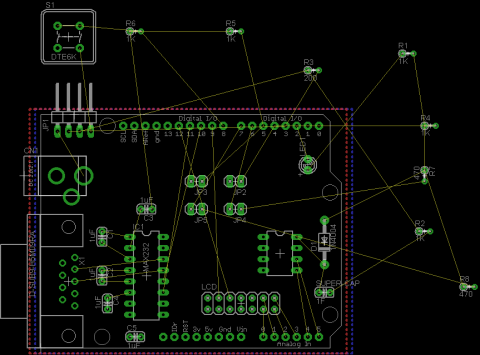
In the above schematic, you can see the pin layouts on the Arduino shield in the upper right (as well as a note that they are no good!)
I will have to delete some of my shield pin assignments and re do them. This is a good lesson for all of you new to schematic layout work:
It is counter intuitive, but you must resist the urge to draw wires from component to component! The reason is that if you need to make a major change, not only is it terribly tedious to redraw all those lines, but you could actually end up removing links you dont intend to remove.
The solution here is to only draw interconnections in small sub circuits. Just like you write code as many small functions, that connect externally with variables and semaphores, you draw schematics as smalls sub sections, with many virtual links.
In Eagle, you will need to make liberal use of the NAME and LABEL commands. NAME will join nets together, while LABEL actually shows those net names on your schematic as gray text.
To repair my schematic, I need only delete the short green lines and dots from the pins on the shield and redraw them, giving them the new name and labels. Actually, you can simply rename them.
I had actually begun to do my component placement and preliminary board traces when I began to realize it was going to be incredibly difficult to route everything. There were a number of reasons for this, as well as a few 'rules' I had broken simply out of being hasty. I know better, I just chose not to consider them. It was late, and I was tired.
You can refer to the following layout as I discuss my mistakes. But be aware, this is actually the SECOND attempt at component placement with the existing schematic! It is AMAZING how resistive your brain is to going back and fixing mistakes rather than just trying to keep fitting that square peg into a round hole. I blame lack of sleep.
I had initially planned on using all of the analog pins for the LCD (since I would not need analog inputs on this project). It made sense. I could keep all of my pins together, leading to a short run to the LCD header. But then I remembered I wanted to slap the real time clock on there, which needs A4 and A5 for I2C SCL and SDA signals. Ok. No problem. I can move the two control pins to Digital pins and keep the data pins on the Analog pins. Great.
WRONG!
The problem with this is that no matter where I placed my LCD header, I would have wires stretched both directions, the full width of the shield. At first this may not seem like a problem. But whenever you have wires that span the full length of one dimension of your board, you have effectively sliced it in half. It becomes VERY difficult to route wires needing to pass across those that bisect the board.
SOLUTION: Move all of the LCD pins to 6 consecutive pins. Or at the very least, pins on both sides, but at one END of the board, so that I can avoid 'cutting off' too much of the pcb with long wires.
The image attached here of the board has already been cleaned up slightly (but obviously will now be abandoned due to a new schematic). Originally, I had placed the real time clock in a different place on the board. It was the only free spot I had found. Once I started routing, I realized I had placed it on the far opposite corner of the A5 and A6 pins! How stupid! The I2C lines had to take long, indirect routes to the chip, and were most certainly of considerably different lengths. This is a big NO NO! You should try to place data/com lines such that the chips are as close as possible, and the lines short and of roughly equal length.
To make matters worse, I had done the same thing to the 232 level converter IC!
SOLUTIONS: Don't lay out boards in the middle of the night, with no sleep! That, and Move your chips around so that they are closest to the pins they connect up to.
In my rush to get the schematic layed out, I found that I did not have the right package for that most basic of parts: a simple push button. The closest match was this huge board space eating monster button (likely really fancy and pretty, but not the simple, tiny tactile switch I was after). No matter. Let's just grab that and move on. I wanna get this done already!
Likely I was already a bit miffed as I had to create the RTC module footprint, and I HATE making footprints. I don't know about you, but I find that Eagle's parts editing system is a total PITA. Anyway, moving on...
So I went about my business.
Now, this is FINE to do, provided you recognize that you WILL have to change the part to the correct footprint BEFORE you start doing pcb layout. I mean, you don't HAVE too, but you will make a lot of assumptions around the WRONG part!
I found myself trying to squeeze everything onto the board, mindful to keep out of this big patch of realestate that ultimately, I would not be needing to preserve anyway!
SOLUTION: Either correct the part before layout, or remind yourself constantly that "YES! I CAN use that board space, because when I get off my ass to fix this part footprint, it will not be so damn huge!"
So I will be spending a few hours to rework the schematic, so that the layout will be much cleaner and far easier to route the pcb.
- See more at: http://diy-scib.org/blog/ths-membership-box-project-planning#sthash.0tfZ...
- See more at: http://diy-scib.org/blog/ths-membership-box-project-planning#sthash.0tfZ...
- See more at: http://diy-scib.org/blog/ths-membership-box-project-planning#sthash.E4Bs...
- See more at: http://diy-scib.org/blog/ths-membership-box-project-planning#sthash.E4Bs...
Theme by Danetsoft and Danang Probo Sayekti inspired by Maksimer